


Almost every year, most of the tech community awaits the evolution of Apple’s A-series cellular system-on-a-chip (SoC), designed primarily by Apple for the iPhone and iPad lineups, to discover innovations introduced in the latest A-series SoC. The iPhone 13 model with the A15 Bionic SoC launched this year is no exception.
These Apple SoC devices use the ARM architecture and are recently built exclusively with TSMC’s most advanced logic process technology. As such, the major technological features observed in Apple’s A-series SoCs are likely to be referred to as landmarks for advances in processor architectures and early adoption of advanced semiconductor manufacturing technologies.
The recently released iPhone 13 model is powered by Apple’s latest A-series chipset, the A15 Bionic SoC, featuring an Apple-designed 64-bit 6-core CPU powered by two high-performance cores and four high energy-efficient cores.
There is already a lot of publicly available information about the cores. The focus of this article is not to discuss the cores, but rather to explore some new features introduced in the A15 SoC, which is manufactured by TSMC using N5P (Performance P) finFET process technology, a second-generation 5nm finFET manufacturing process that is a performance-enhanced version of the 5nm family (N5). This N5P process can allow for additional performance and power improvements.
To understand the correlation between patents and innovations, UnitedLex, a leader in IP and technology, quickly investigated the A15 SoC extracted from the iPhone 13 Pro Max built with TSMC’s one of most advanced process technologies (N5P). Semiconductor patents sometimes require advanced reverse engineering and in-depth technical know-how to fully capture the key device/process characteristics of advanced semiconductor devices to strongly support some custom IP programs.
Structural findings inside the A15 Bionic SoC
A quick target-specific TEM structural analysis allowed us to confirm that the process node used to fabricate the A15 Bionic SoC is the second-generation 5nm (e.g., N5P). Key geometry measurements, including the minimum pitch of each critical layer (e.g., fins, gates, and interconnects), represent a 5nm node finFET process technology family.
As TSMC described, N5P likely continues to incorporate several scaling boosting features as a part of design-technology co-optimization (DTCO) practices in the 5nm process. Scaling boosters are structural modifications without affecting the design rules that improve the performance of the transistor.
Key layout and process features observed include tight diffusion termination (e.g., unique single diffusion break), contact over the active gate (COAG), optimized gate cut after replacement metal gate (RMG) formation and PMOS with SiGe fins for high mobility channels (HMC). It’s not much different from the first generation 5nm technology (N5). There seems to be some fine-tuning in each observed feature to claim a performance boost with N5P technology.
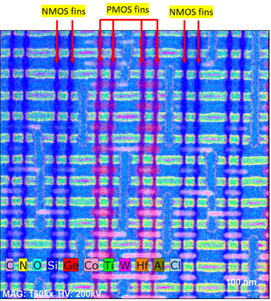
One thing that stands out about this SoC is that traditional single diffusion break (SDB) is rarely observed in some cores (e.g., GPU cores), as seen from the TEM plan view on one of the logic areas in Figure 1. In observed single diffusion break (SDB) designs where the active fins of the cell are continuous, electrical isolation-based SDB may be employed to extend standard logic cell optimization further and improve transistor performance uniformity.
Figure 1: TEM plan view (PV) at logic area (Exhibit A) and TEM PV EDS element mapping (Exhibit B), Source: UnitedLex(1)
Exhibit A:
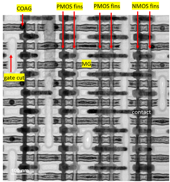
Exhibit B:
Every inter-node technology change adds a few new features, but most process features are similar to the previous node. Figure 2 shows the metal gate cut, which was also observed at the first N5 node. The image on the right in Figure 2 shows a typical fin structure covered with a layer of oxide and high-k dielectric and wrapped with a metal gate as seen since the first finFET devices were introduced.
Figure 2: TEM cross-section across the fin at 6T SRAM (Exhibit 2A) and high-resolution TEM imaging of 5nm fin (Exhibit 2B), Source: UnitedLex (1)
Exhibit 2A:
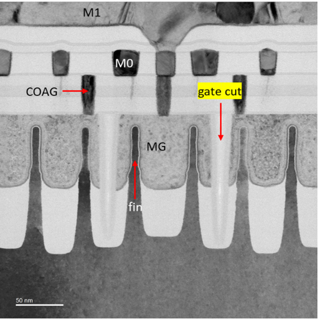
Exhibit 2B:
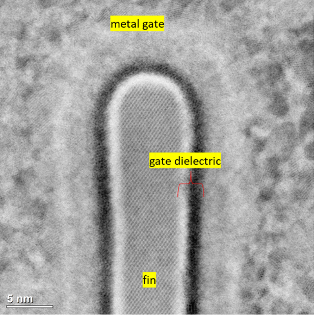
Figure 2: TEM cross-section across the fin at 6T SRAM (Exhibit 2A) and high-resolution TEM imaging of 5nm fin (Exhibit 2B), Source: UnitedLex (1)
In short, since N5P is a process in the N5 family (5nm node variants), the evolution from N5 to N5P doesn’t seem to show a significantly altered process as described above. To find new ways to scale devices, major leading-edge device manufacturers are likely implementing different scaling optimization approaches within the same process node with the help of (DTCO), where the scaling booster is one of the parameters.
The inter-process node improvement approach does not require intensive re-design efforts, allowing foundries to offer their customers multiple options within the same process node. IPs are similar between process node variants. Some keep the N5 while others adopt the N5P or N4, which is an extension of N5, allowing for some performance gains and less power consumption of the device with similar IPs.
Although key process integration and materials are unlikely to change much within the same process node variant, several process architectural scaling boosting capabilities will enable both logic and SRAM density reductions. Process evolution with the same family nodes usually means re-usable IP, some transistor performance optimizations, some critical layer scaling features, some contact/metal layers optimizations, improvements in standard cell layouts, etc.
Finally, no one has a perfect crystal ball for predicting what will happen next with the evolution of advanced logic devices (still “more Moore” or “more than Moore”).
One thing for sure is that all semiconductor manufacturers will evaluate device performance versus economic outcomes before implementing scaling boosters to expand a technology node, migrating to a new technology node, or adopting an entirely new structure. Meanwhile, we at UnitedLex continue to unravel more hidden features of this A15 SoC.
References:
(1). A quick structural overview of Apple’s A15 Bionic SoC fabricated by TSMC 5nm N5P (performance-enhanced version) process, UnitedLex IP Solutions, and Semiconductor Team
Young Min Kwon is a Director of UnitedLex’s IP Solutions group. As a strategic partner, UnitedLex IP team works with the world’s leading technology-focused and semiconductor companies. It offers an unparalleled combination of in-depth technical subject matter expertise, IP experience and reverse engineering.